
About Wafer Dicing at Pin 1 Semiconductor
Every integrated circuit starts as one of hundreds or thousands of die on a wafer. At Pin 1 Semiconductor, our process begins by singulating that wafer into individual die, on four ADT dicing saws in Garnet Valley, Pennsylvania, with capacity up to full 300 mm (12 in) wafers.
- Up to 300 mm (12 in) wafers
- Four ADT dicing saws in-house
- Silicon, GaN, quartz, glass, ceramics, laminates
- Blue PSA or UV-release tape
- Vision alignment and fiducial recognition
- Prototype capability, production capacity
Our Wafer Dicing Process
We can process materials including Silicon, GaN, Quartz, Glass, Ceramics, Laminates and more.
Mount
Wafers are mounted to tape frames, typically on blue PSA tape or UV-release tape. The tape holds the wafer during dicing and holds the die once they are singulated.
Align
Dicing programs are taught using machine vision and fiducial pattern recognition, for accurate alignment on a single wafer and automatic processing of multiple wafers.
Cut
Abrasive diamond resin blades cut through brittle materials with minimal kerf and chipping. Deionized water lubricates the cut and flushes away debris.
Clean
Each wafer is rinsed and dried, then the next wafer is loaded, keeping multi-wafer lots moving.
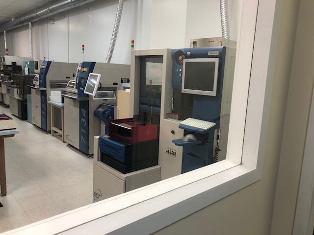
Four ADT Dicing Saws, One Facility
At Pin 1 Semiconductor, wafers are processed on our four ADT wafer saws in Garnet Valley, PA, with capability to process individual die up to full 300 mm (12 in) wafers. Not only do we have capability, but we have production capacity.
- ADT 7124
- ADT 7134
- ADT 7200
- ADT 7222
Wafer Dicing Specifications
Have a requirement that falls outside the table? Contact us chances are we can accommodate it.
| Parameter | Specification |
|---|---|
| Wafer size | Up to 300 mm (12 in) |
| Materials | Silicon, gallium nitride (GaN), quartz, glass, ceramics, laminates |
| Mounting | Tape frame, blue PSA tape or UV-release tape |
| Alignment | Machine vision with fiducial pattern recognition; automatic multi-wafer processing |
| Blades | Diamond resin, for minimal kerf and chipping |
| Coolant | Deionized water (lubrication and debris flushing) |
| Equipment | ADT 7124, 7134, 7200, 7222 |
Wafer Dicing FAQ
What wafer sizes can you dice?
We dice wafers up to full 300 mm (12 in) on four ADT dicing saws in Garnet Valley, PA. Dicing programs are taught with machine vision and fiducial pattern recognition, so we can align a single wafer accurately and process multiple wafers automatically.
What materials can you dice?
We can process materials including silicon, GaN, quartz, glass, ceramics, laminates and more. If your material is not listed, contact us with your requirements.
How are wafers mounted for dicing?
Wafers are mounted to tape frames, typically on blue PSA tape or UV-release tape. The tape holds the wafer during dicing and holds the die after they are singulated.
What dicing equipment and blades do you use?
Our four ADT wafer saws (models 7124, 7134, 7200 and 7222) use abrasive diamond resin blades to cut brittle materials with minimal kerf and chipping. Deionized water lubricates the cut and flushes away debris, and each wafer is rinsed and dried after dicing.
Can you handle production volumes as well as prototypes?
Yes. Not only do we have the capability, we have production capacity: four saws and automatic multi-wafer processing support everything from prototype lots to production runs.
What happens to the die after dicing?
Singulated die can go straight into our in-house die bonding, wire bonding and flip chip assembly services, so your parts move from wafer to assembled device under one roof.
Where is your wafer dicing facility?
Our wafer dicing line is at 3070 McCann Farm Drive, Unit 110, Garnet Valley, Pennsylvania 19060, and we serve customers across the United States.