Service
Die Bonding Services
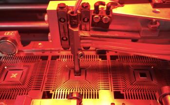
Pin1 Semiconductor runs manual and automated die-attach equipment side by side, so we can scale from single-prototype die placement through medium-volume production on the same floor without re-qualification.
- Silver-filled and non-conductive epoxies
- Solder pre-form and eutectic AuSn die attach
- Sintered silver for high-power thermal paths
- Flip-chip capable die attach stations
- Controlled bond-line thickness (BLT)
- Die placement accuracy to ±5 µm
Capabilities
Process specifications
A snapshot of the parameters our die bonding services line supports. Have a requirement that falls outside the table? Contact us — chances are we can accommodate it.
| Parameter | Specification |
|---|---|
| Die sizes | 0.2 mm² to 20 mm × 20 mm |
| Attach materials | Ag-epoxy, AuSn, Sn-Pb, sintered Ag, non-conductive epoxy |
| Placement accuracy | ±5 µm typical |
| Bondline control | 10 µm to 50 µm controlled BLT |
| Substrates | Open-cavity QFN/QFP, ceramic, leadframe, BGA, PCB |
| Cure profiles | Box oven, in-line IR, vacuum reflow |
| Turnaround | Same-day die-attach available |
Explore more