
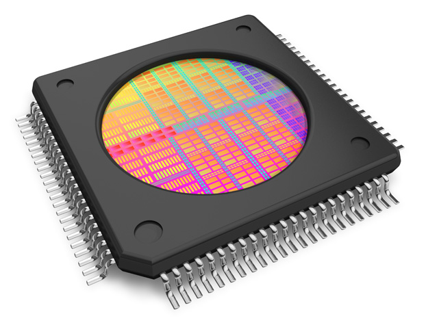
Quick-turn IC assembly & semiconductor packaging
From a single wafer to full production volumes, Pin1 Semiconductor delivers precision wafer dicing, die bonding, wire bonding and flip chip assembly
300 mm
Max wafer size
35 µm
Fine-pitch wire bond
1 piece
Minimum order
Who we are
A US supplier built around speed, precision, and low-volume flexibility
Pin1 Semiconductor LLC is a semiconductor assembly and packaging house based in Garnet Valley, Pennsylvania. We specialize in quick-turn IC assembly for prototype, engineering, and small-volume production programs that large offshore houses cannot economically handle.
Our standard flow — wafer dicing through serialization — with quick turn processing, so fabless startups, universities, defense primes and Tier 1 OEMs can iterate faster without compromising quality.
- Single-piece to full-reel quantities on the same line
- Epoxy, solder and eutectic die-attach under one roof
- Gold ball, aluminum wedge, stud bump & heavy-wire bonding
- Open-cavity QFN/QFP stock for instant prototype packaging
Services
Full-service semiconductor assembly, under one roof
Every step of the IC packaging flow — from bare wafers to packaged integrated circuits.
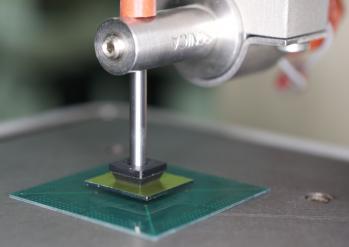
Die Bonding
Epoxy, solder and eutectic die-attach for demanding thermal and electrical paths.
Learn more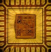
Our process
From bare wafer to marked device
Excellence in Integrated Circuit Assembly.
1
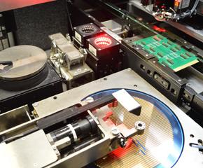
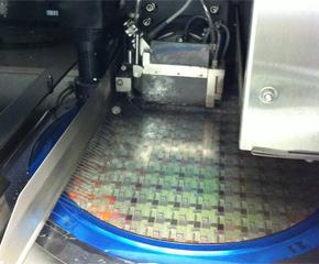
Wafer Dicing
Diamond-blade & laser dicing up to 300 mm
2
Die Attach
Epoxy, solder, eutectic bonding
3
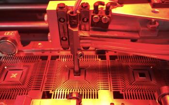
Wire Bonding
Ball, wedge & heavy wire
4
Encapsulation
Transfer mold & glob top
5
Mark & Ship
Serialization, inspection, out the door
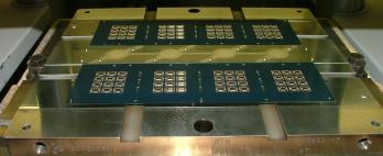
Products
Open-cavity, overmolded, ceramic & custom packages
We stock the most common prototype packages so you can skip long lead times.
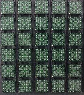
Open Cavity QFN
Stock open-cavity QFN packages for rapid prototype and MEMS assembly.
Open Cavity QFP
Open-cavity QFP / LQFP packages for optical sensors and prototype IC work.
Overmolded Packages
Transfer-molded QFN, QFP and SOIC packages in production volumes.
Ceramic Packages
Hermetic ceramic packages for hi-rel, aerospace and RF applications.
BGA Substrates
BGA substrates, interposers and high-density PCB substrates.
Lids & Seals
Metal, ceramic and glass lids for hermetic and near-hermetic sealing.
Why Pin1
Excellence In IC Assembly
Quick Turnaround
Standard flow — dicing through ink marking — completes the same business day. Critical prototypes can ship the same day.
US-based assembly
US based assembly in Garnet Valley, PA — onshore-reshoring ready.
Prototype to production
The same engineers who build your first 10 units design the process that scales to 10,000. No hand-offs, no re-qualification, no surprises.
Ultra-fine pitch
35-micron wire-bond pitch, stud bumping, and thermosonic gold ball bonding on pads as small as 45 µm.
Open-cavity stock
On-shelf open-cavity QFN, QFP and ceramic packages eliminate 6-to-12 week substrate lead times for your engineering runs.
Full traceability
Lot-level traceability, SPC, destructive and non-destructive bond pull & shear testing supported in-house for qualification programs.
Ready to move your project forward?
From a single wafer to full production runs — our Garnet Valley, PA facility turns your design files into packaged devices. Send us your specs and we’ll quote the same business day.